

Product Brief
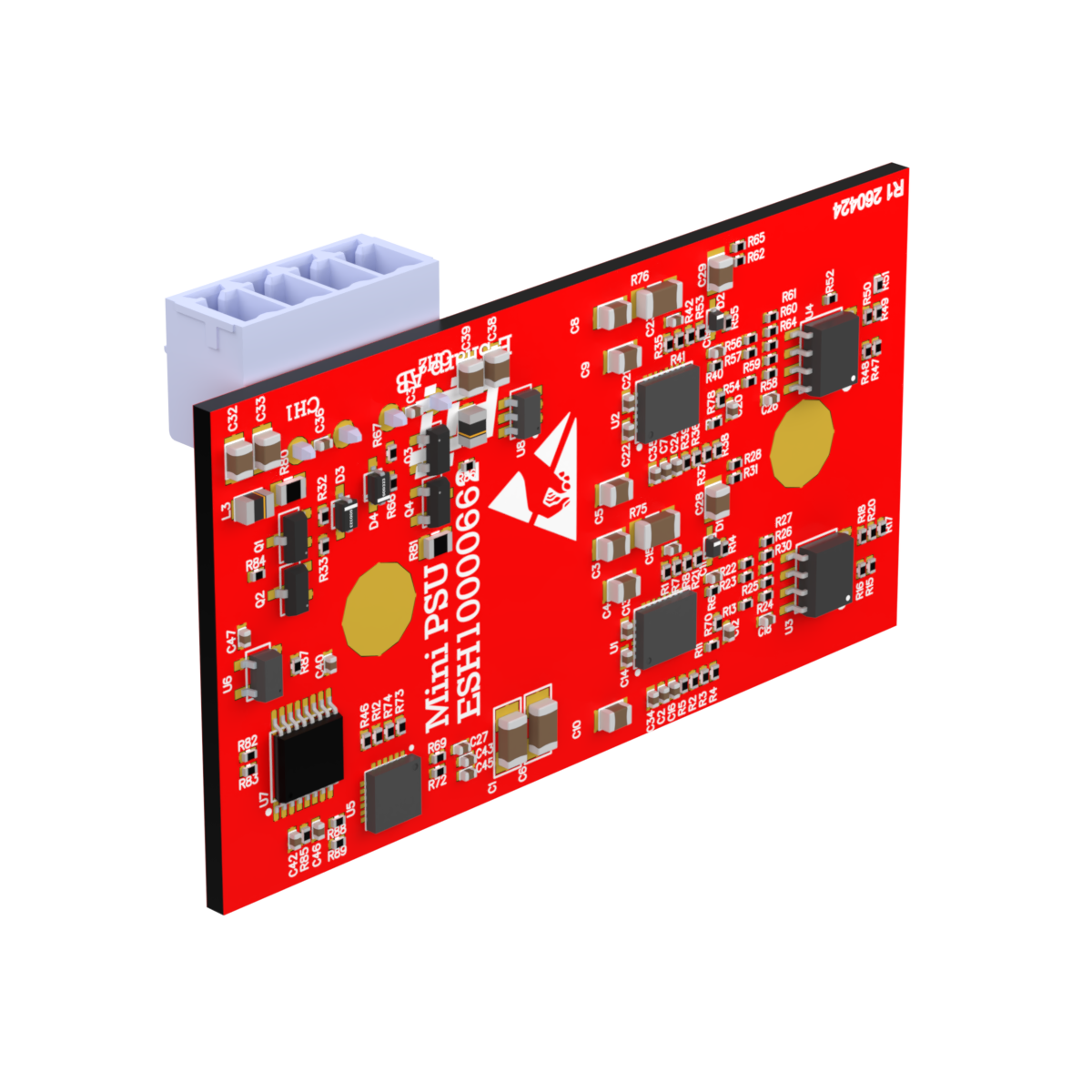
The ESH10000662 is a 2-channel programmable buck-boost power supply in Comtop Module form factor. Each channel delivers a fully independent, regulated output voltage with a programmable constant-current limit. Output voltage and current limit are set via an onboard DAC over I²C, and actual output voltage is monitored via an onboard ADC — all from the same I²C bus. This makes the module suitable for automated test systems that require precision power delivery without requiring per-channel analog control lines.
The converter topology is buck-boost, allowing operation across input voltages both above and below the output setpoint. Hardware overvoltage and undervoltage lockout protect the converter and load from supply excursions.
Key use cases:
-
Programmable power supply in Accordion-based test systems
-
Voltage margin testing and power cycling of DUTs
-
Constant-current load simulation
-
Multi-rail supply in automated production test fixtures
Datasheet
|
Parameter |
Value |
|---|---|
|
Form factor |
Comtop Module |
|
Output channels |
2 (independent) |
|
Output voltage range |
0 V – 24 V per channel |
|
Maximum continuous output current |
1.5 A per channel |
|
Output topology |
Buck-boost |
|
Control interface |
I²C |
|
Voltage setpoint (VSET) |
DAC, 0–4.79 V → 0–24 V (gain ≈ 5.01 V/V) |
|
Current limit setpoint (ISET) |
DAC, 0.20–4.56 V → 0–1.5 A |
|
Current limit linearity |
≤ ±0.1% of full scale (1.5 A) |
|
Output voltage monitoring |
ADC per channel via resistor divider |
|
Current monitoring |
Analog ISMON per channel (buffered, 10× V_sense + 250 mV) |
|
Switching frequency |
~980 kHz |
|
UVLO (input, rising / falling) |
16.7 V / 14.7 V |
|
OVLO (input, rising / falling) |
29.6 V / 28.7 V |
|
Output OVP threshold |
29.4 V |
|
Load transient (0→1.5 A step) |
≤ 1% overshoot; recovery within 5 µs |
|
Long-term output stability |
≤ ±0.1% drift over 8 h at 24 V / 1 A |
|
Thermal limit (full load, 25 °C ambient) |
≤ 50 °C case / PCB hotspot |
|
Per-channel enable |
EN1n / EN2n (active-low) |
|
Per-channel PWM control |
PWM1n / PWM2n (active-low) |
|
Buck-boost controller |
LT3942 |
|
DAC/ADC |
AD5593R (8-channel, 0–5 V full-scale) |
|
GPIO expander |
PI4IOE5V6416 (I²C, address 0x20) |
Manual
Architecture
Each channel is built around an LT3942 4-switch buck-boost controller operating at ~980 kHz. The controller transitions seamlessly between buck, buck-boost, and boost modes based on the ratio of input voltage to output voltage setpoint. Hardware UVLO (16.7 V rising) and OVLO (29.6 V rising) protect the converter against input supply excursions. An output FB overvoltage protection threshold at 29.4 V protects the load.
An AD5593R provides 8 programmable DAC/ADC channels over I²C. DAC channels are used for VSET and ISET per channel; ADC channels are used for VMON (output voltage monitoring via resistor divider) and ISMON (current monitor readback). A PI4IOE5V6416 16-bit GPIO expander (I²C address 0x20) handles digital control signals: EN1n/EN2n and PWM1n/PWM2n.
Voltage Control
Output voltage is set by writing the VSET DAC channel for each output. The DAC output feeds a gain network (OPA2192 op-amp) before the LT3942 FB pin.
|
Parameter |
Value |
|---|---|
|
DAC full-scale |
5 V (AD5593R, VDD-referenced) |
|
Maximum VSET |
4.79 V (firmware cap) |
|
Output voltage at VSET = 4.79 V |
24.0 V |
|
Voltage gain |
≈ 5.01 V/V |
|
FB regulation target (LT3942) |
1.00 V ± 1.5% |
Current Limit Control
Constant current limit is set by writing the ISET DAC channel. The DAC output is scaled via a resistor network to the LT3942 CTRL pin.
|
Parameter |
Value |
|---|---|
|
ISET active range |
0.20 V – 4.56 V |
|
Current at ISET = 4.56 V |
1.5 A (firmware cap) |
|
Sense resistor (R75/R76) |
50 mΩ |
|
CC linearity |
≤ ±0.1% of full scale |
|
DAC resolution |
≈ 0.42 mA/step (3,571 usable steps) |
The LT3942 enters constant current mode automatically when the output current reaches the CTRL-programmed threshold. In the linear range (VCTRL 0.25–1.15 V), I_IS(MAX) = (VCTRL − 0.25 V) / (10 × 50 mΩ).
Output Monitoring
Output voltage and current monitor values are read back over I²C via the AD5593R ADC:
|
Signal |
Source |
Description |
|---|---|---|
|
VMON1 / VMON2 |
AD5593R ADC |
Output voltage via resistor divider |
|
ISMON1 / ISMON2 |
AD5593R ADC |
LT3942 ISMON: |
Enable and PWM Control
Each channel has an active-low enable signal and an active-low PWM control signal, routed through the PI4IOE5V6416 GPIO expander.
|
Signal |
Type |
Description |
|---|---|---|
|
EN1n |
Active-low output |
Enable Channel 1 — assert low to enable |
|
EN2n |
Active-low output |
Enable Channel 2 — assert low to enable |
|
PWM1n |
Active-low output |
PWM control for Channel 1 (5 V pull-up) |
|
PWM2n |
Active-low output |
PWM control for Channel 2 (5 V pull-up) |
GPIO expander init sequence: Write output register (02h/03h) before setting pin direction (06h/07h) to prevent glitch on enable lines. Pull resistors are disabled by default — drive all outputs explicitly at startup.
Protection
|
Protection |
Mechanism |
Threshold |
|---|---|---|
|
Input undervoltage lockout |
LT3942 EN/UVLO |
Rising: 16.7 V; Falling: 14.7 V |
|
Input overvoltage lockout |
LT3942 OVLO |
Rising: 29.6 V; Falling: 28.7 V |
|
Output overvoltage protection |
LT3942 FB OVP |
29.4 V |
|
Soft-start |
LT3942 SS pin |
~1.76 ms ramp (CSS = 22 nF) |
|
Fault mode |
SS → VREF via 100 kΩ |
Keep-running (no latch-off, no hiccup) |
I²C Device Map
|
Device |
Address |
Function |
|---|---|---|
|
AD5593R |
[TODO: confirm] |
VSET1/VSET2 DAC, ISET1/ISET2 DAC, VMON1/VMON2 ADC, ISMON1/ISMON2 ADC |
|
PI4IOE5V6416 |
0x20 |
EN1n/EN2n, PWM1n/PWM2n, auxiliary GPIO |
Pinout
J2 – Output Connector (Phoenix, 4-pin)
|
Pin |
Signal |
Description |
|---|---|---|
|
1 |
VOUT1 |
Channel 1 output voltage |
|
2 |
GND |
Output ground |
|
3 |
GND |
Output ground |
|
4 |
VOUT2 |
Channel 2 output voltage |
| Version | Date | Comment |
|---|---|---|
| Current Version (v. 3) | May 08, 2026 15:21 |
@User
|
| v. 2 | Apr 27, 2026 18:00 |
@User
|
| v. 1 | Apr 27, 2026 17:59 |
@User
|